|
 |
OK, so this is what I have. I'm still debugging it, but it should more
or less work now.
It's an 8-bit processor. All data paths are 8 bits wide. There are three
general-purpose registers, named X, Y and Z. They're all 8 bits wide.
Since the address bus is also 8-bit, the processor is limited to a
piffling 256 bytes of addressible memory (unless you go implement
banking). There are 17 valid opcodes (plus more which may or may not
produce predictable results.)
All instructions are exactly 2 bytes long. The first byte is an opcode,
and the second is a memory address (which may or may not actually be
used for anything). It's merely simpler to design if all instructions
use an identical addressing mode. Similarly, all instructions are
exactly 6 clock cycles long, even if some of them could actually be done
faster.
There are basically 4 instructions:
- Unconditional load.
- Conditional load.
- Save.
- Math-op.
A conditional load does exactly the same thing is an unconditional load
*if* the last math-op produced a result exactly equal to zero. Otherwise
an unconditional load does nothing at all.
Either way, a load copies the contents of the specified memory register
into one of the internal registers. Since the target register can be the
Program Counter, an unconditional load instruction can be used to
perform an unconditional jump (to an absolute address). Similarly, a
conditional load can perform a conditional jump.
A save instruction does the reverse: it copies the contents of the
specified register (including the PC) to the specified memory address.
There are 5 possible math-ops. They all take X and Y as their operands,
and store their result in Z. (They also set or clear the "zero flag"
that the conditional load instruction tests.) The available operations
are bit-wise AND, OR, XOR, binary addition and binary subtraction.
Currently math-ops generate several flags, but it is impossible to
access any of them except the zero flag. In particular, this means that
16-bit addition would be spine-tinglingly difficult to implement in
software. What I probably need to do is utilise some of the unused bits
in the opcode to select what condition the conditional load instruction
tests. (Which means *another* binary decoder in the control matrix...)
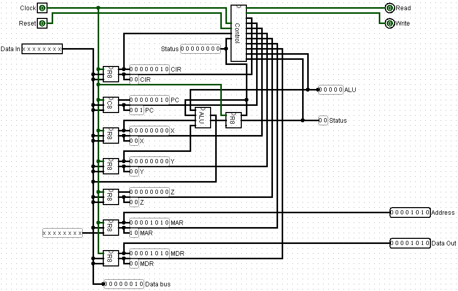
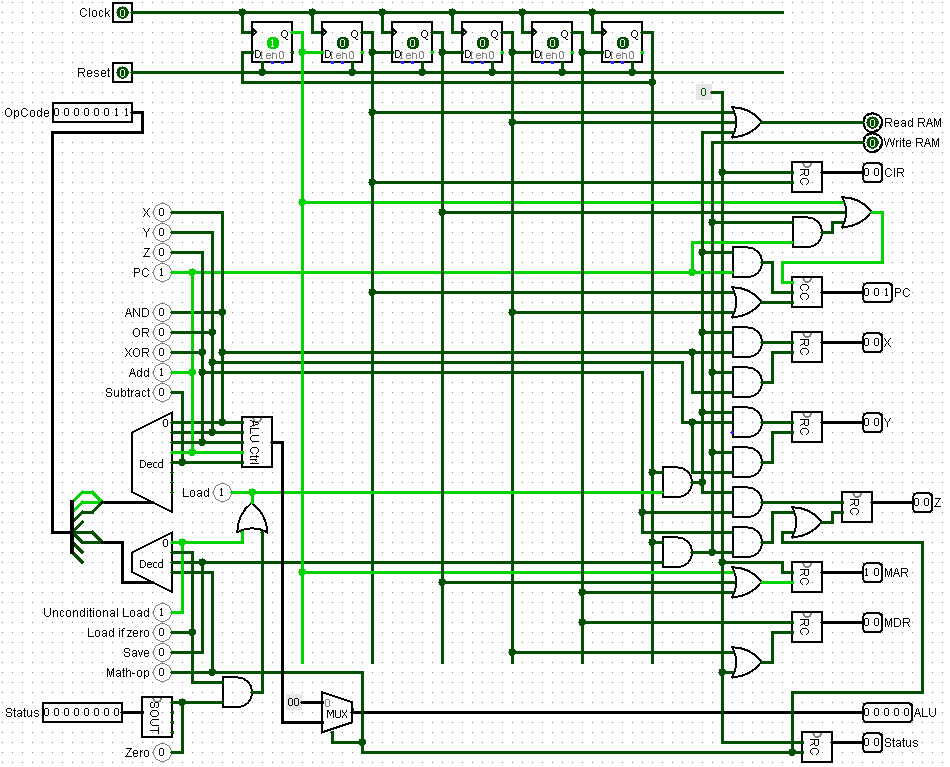
As you can see, the CPU itself is quite simple; just a bunch of
registers attached to a single common data bus. The complexity comes
from the maze of control busses eminating from the control matrix. And
when you look inside the control matrix itself... woah. OK, that's
pretty complicated! o_O
Now, if I can just figure out a reasonable way of getting Logisim to
test the damned thing...
Post a reply to this message
Attachments:
Download 'processor.png' (13 KB)
Download 'control matrix.png' (23 KB)
Preview of image 'processor.png'
Preview of image 'control matrix.png'
|
|